Introduction to Semiconductor Devices
Semiconductor devices are electronic components made from semiconductor materials, primarily silicon, germanium, or compound semiconductors like gallium arsenide. These materials have conductivity between that of insulators and conductors, which can be controlled by doping—adding impurities to create excess electrons (n-type) or electron deficiencies called holes (p-type). The behavior of these devices relies on the movement of charge carriers (electrons and holes) under electric fields, light, or other stimuli. Below, I’ll explain the working principles of some key semiconductor devices.
PN Junction Diode

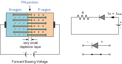
Source: electronics-tutorials.ws
A PN junction diode is formed by joining p-type and n-type semiconductors, creating a depletion region at the interface where mobile charges recombine, leaving immobile ions that form a built-in electric field.
In forward bias (positive voltage to p-side, negative to n-side), the external voltage reduces the depletion region’s barrier, allowing majority carriers (holes from p-side, electrons from n-side) to cross and recombine, enabling current flow. This recombination releases energy, but in a standard diode, it’s mostly heat.
In reverse bias (opposite polarity), the barrier increases, preventing significant current flow except for a small leakage current from minority carriers. Diodes are used for rectification, converting AC to DC, and in signal clipping or protection circuits.
Bipolar Junction Transistor (BJT)

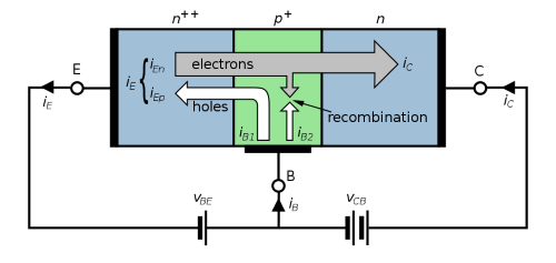
A BJT is a three-layer device, typically NPN (n-p-n) or PNP (p-n-p), with terminals called emitter, base, and collector. It acts as a current amplifier or switch.
In an NPN BJT, a small base-emitter current (forward bias on base-emitter junction) injects electrons from the emitter into the thin base region. Most of these electrons diffuse across the base to the collector (reverse-biased base-collector junction), creating a larger collector current. The base current controls the collector current, with amplification factor β (beta) typically 50-200.
In active mode, it’s used for amplification; in saturation, as a switch (on); in cutoff, as off. BJTs are fundamental in analog circuits like amplifiers and digital logic.
Metal-Oxide-Semiconductor Field-Effect Transistor (MOSFET)

A MOSFET is a voltage-controlled device with source, drain, gate, and body terminals. It consists of a semiconductor channel between source and drain, separated from the gate by a thin oxide layer.
In an n-channel enhancement-mode MOSFET (common type), applying a positive gate-source voltage creates an electric field that attracts electrons to the p-type body under the gate, forming an inversion layer (n-channel) that connects source and drain. This allows current to flow from drain to source when a drain-source voltage is applied.
The gate voltage modulates the channel conductivity without drawing significant current (high input impedance). MOSFETs are widely used in digital ICs (like CMOS logic), power switching, and amplifiers due to their efficiency and scalability.
Light-Emitting Diode (LED)

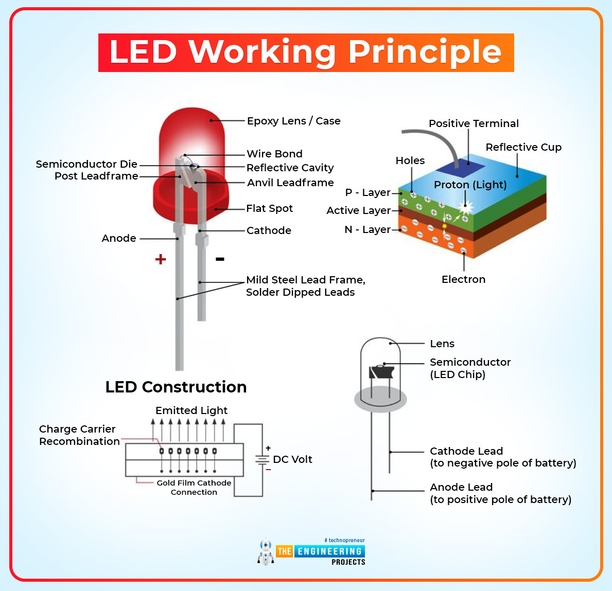
An LED is a PN junction diode made from direct-bandgap semiconductors (e.g., GaAsP for red light). When forward-biased, electrons from the n-side and holes from the p-side recombine in the active region.
In LEDs, this recombination releases energy as photons (light) rather than heat, due to the material’s bandgap matching visible or infrared wavelengths. The color depends on the bandgap energy (E = hc/λ, where λ is wavelength).
LEDs require a forward voltage drop (typically 1.8-3.3V depending on color) and a current-limiting resistor. They’re used in displays, lighting, and indicators for their efficiency and longevity.
Solar Cell (Photovoltaic Cell)

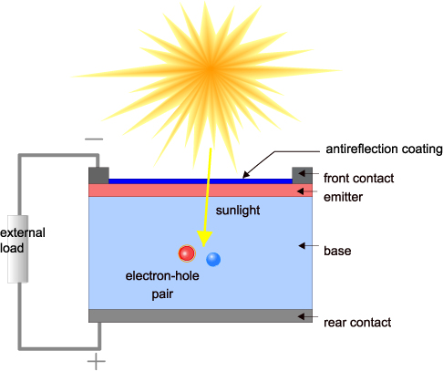
A solar cell is a PN junction designed to convert light into electricity via the photovoltaic effect. Incident photons with energy greater than the bandgap generate electron-hole pairs in the depletion region or nearby.
The built-in electric field separates these carriers: electrons to the n-side, holes to the p-side, creating a voltage across the junction. When connected to a load, this drives a current.
Efficiency depends on material (e.g., silicon ~15-20%), anti-reflective coatings, and design. Solar cells are used in panels for renewable energy, powering everything from calculators to grids.